There is the short description of my old 23cm transverter :
I am using home built transverter of my own construction, the transverter is was designed as modular construction and divided on four main modules:
1. Receiver module
2. Transmitter module
3. Local Oscillator (PLL) module
4. OCXO 10MHz – reference clock module
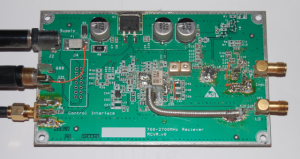
1. Recever
The receiver schematic you can see on my Download page
From beginning RX module was designed as RF part of Sound Card based SDR, i.e. direct conversion of 1296Mhz signal to I/Q audio IF and further processing on Personal Computer SDR software. But in reality it was hard to struggle against Local Oscillator leakage and phase noise, so I decided to leave this idea and to use it as 1296Mhz/28Mhz converter. So now two I and Q channel are adding together, after simple 28Mhz RF phase shifting RC network, this gives additional attenuation of image channel (the main filtering is done in input 1296Mhz helical filter).
Second issue with this RX design it is – input LNA it is exact copy of input stage of DB6NT transverter. Because I was unlucky to get from this LNA noise figure better than 3dB, plus poor stability (existence of higher band microwave oscillations) , decided to change both amplifiers stages and now I am using there ATF51343 as input amplifier and GALI39 as second stage amplifier. It give me no oscillation and NF=1.5dB, that is good enough for system that using additional LNA on the antenna feed. Please, pay attention, the RX module schematic, that is located in Download area, contains only old LNA design. I need some time, to prepare electronic copy of my, hand written, changes to schematic 🙂